VLSI DESIGN - Set Input/Output Delays
Timing closure is one of the most critical aspects of digital circuit design. When working with hierarchical designs. This blog will introduce the concept of input/output delays and how to set them properly set them in block/top level design.
Understanding Input and Output Delays
In digital circuit design, input and output delays are critical timing constraints that inform synthesis and implementation tools about external circuit delays outside the current design block’s visibility. Understanding how input/output delays affect setup/hold constraints is fundamental for achieving proper timing closure in your design.
Setup and Hold Timing Constraints
setup timing is defined as the time window during which the data must be stable before the clock edge, while hold timing is the time window during which the data must remain stable after the clock edge, the equation is:
where:
- $T_{\text{clk}}$ is the clock period
- $T_{\text{clk_launch}}$ is the clock launch time
- $T_{\text{clk_capture}}$ is the clock capture time
- $T_{\text{comb_path}}$ is the combinational path delay
- $T_{\text{c2q}}$ is the clock-to-Q delay (propagation delay from clock edge to output change, not considered in subsequent examples)
Analysis of output delay
For FF2 in Figure 1, following above equations, we have:
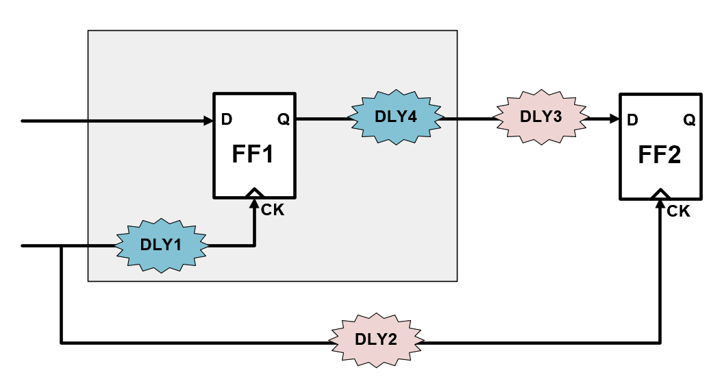
Since output_delay is calculated as:
we can rewrite the equations as:
\[\begin{align} T_{setup} &= T_{clk} - \text{DLY1} - \text{DLY4} - T_{\text{output\_delay}} \\ T_{hold} &= \text{DLY1} + \text{DLY4} + T_{\text{output\_delay}} \end{align}\]Analysis of input delay
For FF1 in Figure 2, following above equations, we have:
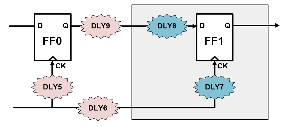
Since input_delay is calculated as:
we can rewrite the equations as:
\[\begin{align} T_{setup} &= T_{clk} + \text{DLY7} - (\text{DLY8} + T_{\text{input\_delay}}) \\ T_{hold} &= \text{DLY8} - \text{DLY7} + T_{\text{input\_delay}} \end{align}\]Practical Examples of Setting Input/Output Delays
Example 1: Block-Level Design (Hierarchical Design)
In a hierarchical implementation flow, when partitioning blocks before clock tree synthesis (CTS), the external clock delay is unknown, i.e., $\text{DLY2}$ and $\text{DLY5}, \text{DLY6}$ in Figure 1 and Figure 2 are unknown. Then we should only consider constraining the input_delay/output_delay on the data path when partitioning blocks.
In our examples, we need to allocate the delays proportionally to the external and internal logic:
- Calculate total available time (clock period)
- Estimate relative complexity of external vs. internal paths
- Allocate delays proportionally
For a design with:
- Clock period: 15ns
- External logic: ~10 buffers of delay
- Internal logic: ~5 buffers of delay
- In Figure 1, the external logic is
DLY3while the internal logic isDLY4;- In Figure 2, the external logic is
DLY9while the internal logic isDLY8;
Calculate budget:
- External delay budget: 10ns (⅔ of period)
- Internal delay budget: 5ns (⅓ of period)
1. Create constraints in the sdc file
Thus, for the sdc file, we have:
1
2
3
4
5
6
7
8
9
# Create actual clock
create_clock -name clk [get_ports ck] -period 15 -waveform {0 7.5}

# Create virtual clock for I/O constraints
create_clock -name vclk -period 15 -waveform {0 7.5}

# Set input/output delay based on budget
set_input_delay  10 [get_ports port1] -clock vclk
set_output_delay 10 [get_ports port2] -clock vclk
2. Enable update_io_latency in PnR tool (Innovus)
Since we didnt consider the clock tree delay in the sdc file, we need to enable update_io_latency in the PnR tool to adjust the I/O delays based on the internal clock tree latency after CTS.
When update_io_latency is enabled, Innovus annotates a negative clock tree latency value (DLY1, DLY7) on the block’s clock port to compensate for internal clock distribution delays.
This behavior exists because the top-level CTS, which occurs after block-level design, ensures balanced clock arrival times at all flip-flops (FF0, FF1, and FF2). For instance, in Figure 2, the top-level CTS will balance the delays such that DLY5 ≈ DLY6 + DLY7. During block-level design, while DLY5 and DLY6 are considered zero, the tool calculates an internal clock tree latency for DLY7. To maintain the equation DLY5 + DLY7 ≈ DLY6 + DLY7, update_io_latency will let the tool annotate a negative value equal to DLY7 on the block’s clock port, compensating for the internal clock tree delay.
Example 2: Top-Level Design (Flat Design)
If we go with Top-Level Design, it should NOT enable update_io_latency in the PnR tool, since now the external delays are known and should be correctly included in the input_delay/output_delay values.
We can now calculate the output_delay and input_delay according to equations Equation-output-delay and Equation-input-delay. Then set them in the sdc file.
In mixed-signal designs, where the analog portion typically serves as the top-level design and encapsulates the digital components,
update_io_latencyshould remain disabled in the digital block’s PnR tools. This is because, similar to pure digital flat designs, the external delays are known and should be properly accounted for in the input/output delay constraints.
Conclusion
Setting appropriate input and output delays is crucial for achieving timing closure in VLSI digital designs. The key points to remember are:
- For hierarchical (block-level) designs:
- Budget delays between external and internal paths based on relative complexity
- Enable update_io_latency in PnR tools to handle clock tree delays
- Use virtual clocks for I/O constraints
- For flat(top-level)/mixed-signal designs:
- Disable update_io_latency since external delays are known
- Calculate actual input/output delays using the provided equations
- Account for clock tree delays directly in constraints
Hope this blog helps you to understand how to set input/output delays in different design levels.
Is this blog helpful? Help fuel more in-depth technical content by treating me to a coffee! Your support keeps the knowledge flowing ☕✨
